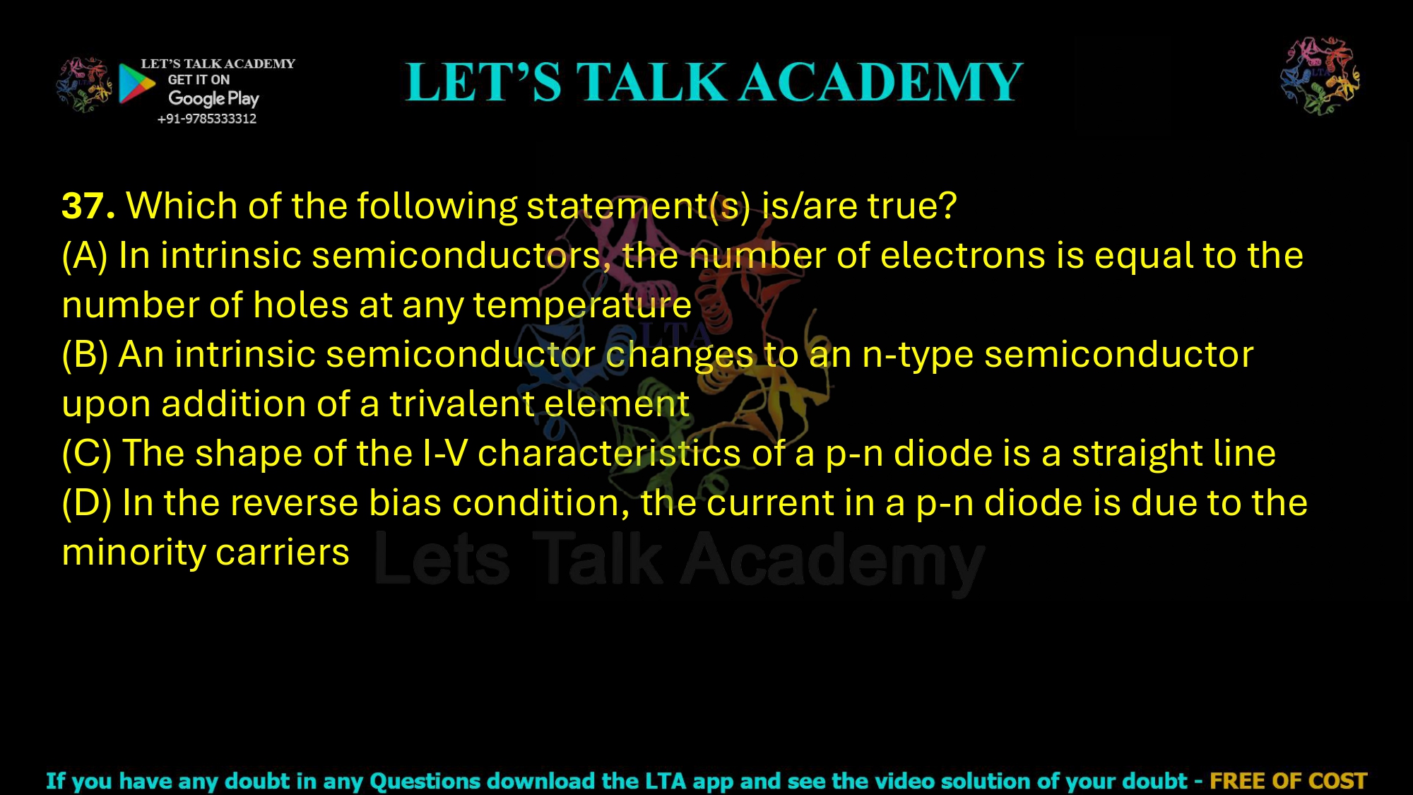
37. Which of the following statement(s) is/are true?
(A) In intrinsic semiconductors, the number of electrons is equal to the number of holes at any temperature
(B) An intrinsic semiconductor changes to an n-type semiconductor upon addition of a trivalent element
(C) The shape of the I-V characteristics of a p-n diode is a straight line
(D) In the reverse bias condition, the current in a p-n diode is due to the minority carriers
Intrinsic Semiconductors and P-N Diode Characteristics: Correct Statements Explained
Correct Answer: (A) and (D)
Understanding the Basic Concepts of Semiconductors and P-N Diodes
This question tests several fundamental concepts of semiconductor physics, including the behavior of charge carriers in an intrinsic semiconductor, the effect of adding impurities to a pure semiconductor, the current-voltage characteristics of a p-n junction diode and the origin of current under reverse-bias conditions.
To identify the correct statements, each option must be examined independently. Statement (A) deals with the relationship between the number of free electrons and holes in an intrinsic semiconductor. Statement (B) concerns the type of semiconductor produced by adding a trivalent impurity. Statement (C) asks whether a p-n diode behaves like an ohmic resistor with a straight-line I-V graph, while statement (D) focuses on the carriers responsible for reverse current.
The correct statements are (A) and (D). In an intrinsic semiconductor, electrons and holes are generated in equal numbers, while the small reverse current in a p-n junction diode is primarily due to minority carriers.
What Is an Intrinsic Semiconductor?
An intrinsic semiconductor is a pure semiconductor material without any intentionally added impurity. Silicon and germanium are common examples of semiconductor materials that can behave as intrinsic semiconductors when they are sufficiently pure.
At absolute zero temperature, the valence band of an ideal intrinsic semiconductor is completely filled and the conduction band is empty. Therefore, there are no free charge carriers available for ordinary electrical conduction.
When the temperature rises above absolute zero, thermal energy can break some covalent bonds. An electron then gains sufficient energy to move from the valence band to the conduction band. The departure of this electron leaves behind an empty state called a hole.
Thus, every thermally generated conduction electron is accompanied by the creation of one hole. Electrons and holes are therefore produced in pairs in an intrinsic semiconductor.
Electron and Hole Concentrations in an Intrinsic Semiconductor
For an intrinsic semiconductor in thermal equilibrium, the electron concentration is equal to the hole concentration:
n = p = ni
where n represents the concentration of free electrons in the conduction band, p represents the concentration of holes in the valence band and ni is the intrinsic carrier concentration.
As temperature increases, more covalent bonds break and more electron-hole pairs are generated. Therefore, the number of electrons and holes both increase. However, because every excited electron creates one corresponding hole, their concentrations remain equal.
At absolute zero, both carrier concentrations ideally become zero, so they are still equal. Therefore, under the usual ideal equilibrium description of an intrinsic semiconductor, the number of electrons is equal to the number of holes at any temperature.
Why Statement (A) Is Correct
Statement (A) says that in intrinsic semiconductors, the number of electrons is equal to the number of holes at any temperature. This statement is correct for an ideal intrinsic semiconductor in thermal equilibrium.
The fundamental reason is that electrons and holes are generated in pairs. Whenever sufficient thermal energy excites an electron from the valence band into the conduction band, one free electron appears in the conduction band and one hole is simultaneously created in the valence band.
Therefore:
Number of free electrons = Number of holes
or, in terms of carrier concentrations:
n = p = ni
The actual value of the intrinsic carrier concentration changes strongly with temperature, but the equality between electron and hole concentrations is maintained.
Understanding Doping in Semiconductors
Pure intrinsic semiconductors generally have relatively low electrical conductivity. Their conductivity can be increased significantly by adding a very small and controlled amount of impurity atoms. This process is known as doping.
The semiconductor produced after doping is called an extrinsic semiconductor. Depending on the valency of the impurity atom added, the semiconductor becomes either n-type or p-type.
Pentavalent impurities produce n-type semiconductors, whereas trivalent impurities produce p-type semiconductors. Understanding this distinction is essential for evaluating statement (B).
Effect of Adding a Trivalent Impurity
A trivalent element has three valence electrons. Examples include boron, aluminium, gallium and indium. When a trivalent impurity atom is added to a tetravalent semiconductor such as silicon or germanium, it can form only three complete covalent bonds with neighboring semiconductor atoms.
One bond remains incomplete because the impurity atom lacks a fourth valence electron. This deficiency behaves like a hole and can accept an electron from a neighboring bond.
For this reason, trivalent impurities are called acceptor impurities. Doping an intrinsic semiconductor with a trivalent element produces a p-type semiconductor, not an n-type semiconductor.
In a p-type semiconductor, holes are the majority carriers, while electrons are the minority carriers.
Why Statement (B) Is Incorrect
Statement (B) claims that an intrinsic semiconductor changes to an n-type semiconductor upon the addition of a trivalent element. This statement is incorrect.
A trivalent impurity creates holes and converts the intrinsic semiconductor into a p-type semiconductor. The majority carriers in the resulting material are holes.
An n-type semiconductor is produced by adding a pentavalent impurity, such as phosphorus, arsenic or antimony. A pentavalent atom has five valence electrons. Four electrons participate in covalent bonding, while the fifth electron becomes relatively free and contributes to electrical conduction.
Therefore:
Trivalent impurity → p-type semiconductor
Pentavalent impurity → n-type semiconductor
Hence, statement (B) is false.
Understanding the I-V Characteristics of a P-N Junction Diode
The I-V characteristic of a device shows how the current through the device changes as the applied voltage is varied. For an ohmic resistor of constant resistance, Ohm’s law gives a direct proportionality between current and voltage.
For an ideal ohmic resistor:
I ∝ V
Therefore, the I-V graph of an ohmic resistor is a straight line passing through the origin.
A p-n junction diode behaves very differently. Its current does not increase linearly with applied voltage. The diode has different behaviors under forward-bias and reverse-bias conditions, producing a strongly nonlinear I-V characteristic.
Forward-Bias I-V Characteristic of a P-N Diode
In forward bias, the p-side of the diode is connected to the positive terminal of the external voltage source, while the n-side is connected to the negative terminal. The applied voltage reduces the width of the depletion region and lowers the potential barrier across the junction.
At small forward voltages, the current remains relatively low. Once the applied voltage becomes sufficiently large, the current increases very rapidly with a small further increase in voltage.
This rapid nonlinear rise in current means that the forward-bias I-V curve is not a straight line. A p-n junction diode therefore does not obey Ohm’s law in the same way as a resistor of constant resistance.
Reverse-Bias I-V Characteristic of a P-N Diode
In reverse bias, the p-side is connected to the negative terminal and the n-side is connected to the positive terminal of the external voltage source. The depletion region becomes wider, and the potential barrier increases.
The majority carriers are pulled away from the junction, so they cannot produce a significant current across the diode. However, a very small current still flows because thermally generated minority carriers can cross the junction under the influence of the electric field.
This reverse current remains nearly constant over a range of reverse voltages until the breakdown region is reached. At breakdown, the reverse current rises sharply.
Therefore, the complete I-V characteristic of a p-n junction diode is clearly nonlinear.
Why Statement (C) Is Incorrect
Statement (C) says that the shape of the I-V characteristics of a p-n diode is a straight line. This statement is incorrect.
A straight-line I-V characteristic is associated with an ohmic conductor whose resistance remains constant. A p-n junction diode is a nonlinear device. Its resistance depends on the applied voltage and the direction of biasing.
In forward bias, the current increases rapidly after the applied voltage becomes sufficiently large. In reverse bias, only a small reverse current flows before breakdown. Therefore, the diode’s I-V characteristic is curved rather than a straight line.
Majority and Minority Carriers in Semiconductors
To understand reverse current in a p-n diode, it is important to distinguish between majority carriers and minority carriers.
In a p-type semiconductor, holes are present in much larger numbers and are therefore the majority carriers. Electrons are present in much smaller numbers and are called minority carriers.
In an n-type semiconductor, electrons are the majority carriers, while holes are the minority carriers.
Therefore:
p-type semiconductor: Holes are majority carriers and electrons are minority carriers
n-type semiconductor: Electrons are majority carriers and holes are minority carriers
These minority carriers play the central role in producing the small current that flows through a reverse-biased p-n junction diode.
Origin of Current in a Reverse-Biased P-N Diode
Under reverse-bias conditions, the applied electric field increases the potential barrier and widens the depletion region. Majority carriers are pulled away from the junction and cannot easily cross it.
However, thermal energy continuously generates a small number of minority carriers in the semiconductor. Electrons that are minority carriers on the p-side and holes that are minority carriers on the n-side can reach the depletion region.
The strong electric field across the depletion region quickly sweeps these minority carriers across the junction. Their motion produces a small reverse current, often called the reverse saturation current.
Thus, the current in a reverse-biased p-n diode is primarily due to minority carriers.
Why Statement (D) Is Correct
Statement (D) says that in the reverse-bias condition, the current in a p-n diode is due to minority carriers. This statement is correct.
Reverse bias prevents the majority carriers from crossing the junction in significant numbers. The small current that remains is produced by thermally generated minority carriers moving across the depletion region under the influence of the junction electric field.
Therefore, reverse current in a p-n junction diode is a minority-carrier current, making statement (D) true.
Detailed Analysis of Each Option
Option (A): In Intrinsic Semiconductors, the Number of Electrons Is Equal to the Number of Holes at Any Temperature
Option (A) is correct. In an ideal intrinsic semiconductor at thermal equilibrium, electrons and holes are generated in pairs. Whenever an electron moves from the valence band to the conduction band, one hole is created in the valence band.
Therefore, the electron and hole concentrations remain equal:
n = p = ni
The carrier concentration changes with temperature, but the equality between electrons and holes remains valid.
Option (B): An Intrinsic Semiconductor Changes to an N-Type Semiconductor upon Addition of a Trivalent Element
Option (B) is incorrect. A trivalent impurity has only three valence electrons and creates an electron deficiency or hole when introduced into a tetravalent semiconductor.
Therefore, a trivalent impurity converts an intrinsic semiconductor into a p-type semiconductor. To produce an n-type semiconductor, a pentavalent impurity must be added.
Option (C): The Shape of the I-V Characteristics of a P-N Diode Is a Straight Line
Option (C) is incorrect. A p-n junction diode is a nonlinear device and does not obey Ohm’s law with a constant resistance.
Its current changes nonlinearly with applied voltage. The forward current rises rapidly after sufficient forward bias is applied, while only a small reverse current flows before breakdown. Therefore, its I-V characteristic is not a straight line.
Option (D): In Reverse Bias, the Current in a P-N Diode Is Due to Minority Carriers
Option (D) is correct. Reverse bias prevents the majority carriers from crossing the junction. The small reverse current is produced mainly by thermally generated minority carriers that are swept across the depletion region by the electric field.
Therefore, the current in a reverse-biased p-n diode is due to minority carriers.
Comparison of Intrinsic, P-Type and N-Type Semiconductors
In an intrinsic semiconductor, the concentrations of electrons and holes are equal. Neither type of charge carrier is present in greater concentration than the other.
In a p-type semiconductor, a trivalent impurity is added. Holes become the majority carriers, while electrons become the minority carriers.
In an n-type semiconductor, a pentavalent impurity is added. Electrons become the majority carriers, while holes become the minority carriers.
This classification is fundamental to understanding the operation of p-n junction diodes, transistors and many other semiconductor devices.
Final Answer
Statement (A) is true because an intrinsic semiconductor has equal concentrations of electrons and holes:
n = p = ni
Statement (B) is false because a trivalent impurity produces a p-type semiconductor, not an n-type semiconductor.
Statement (C) is false because the I-V characteristic of a p-n junction diode is nonlinear and is not a straight line.
Statement (D) is true because the reverse current in a p-n diode is mainly due to minority carriers.
Therefore, the correct statements are (A) and (D).


